|
VLSI TECHNOLOGY LABORATORY
Fabrication Lab was setup in the year 2007 as an integral part of the department of Microelectronics (MI), Followed by commencement of Post Graduation (M.Tech) and Ph.D. programme in the field of Microelectronics subsequently.
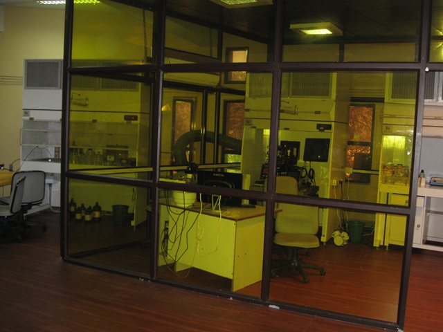
Ever since its inscription the Fabrication lab has constantly been upgraded to match with the technologies of the modern era. The laboratory helps the students, researchers and all enthusiasts to acquire all the much needed concepts to deal with different practical experiments. Laboratory consists of the comprehensive facilities for the fabrication and testing of silicon microcircuits of small to medium complexity, housed in a moderate clean room environment maintaining class 1000 conditions. The laboratory comprises of four sections viz. Wafer Cleaning & Etching, Oxidation & Diffusion, Photolithography, Thin Film / Metal Deposition and Device Characterization. The vision that lead to the inception of this venture have so far been achieved to a great extent and will always be tried to.
Oxidation and Diffusion Section
- Consists of three high temperature (∼1300°C) furnaces, one is for the purpose of thermal oxidation and two others are for the purpose of the diffusion of p- and n-type dopants.
- Three clean benches facility during the loading and unloading of the wafers.
Wafer Cleaning and Etching Section
- Two or three clean benches to create clean environment locally.
- Ultrasonic bath for wafer cleaning and a spinner with IR lamp for drying the wafers are part of this lab.
- Water purification RO and DI water systems for the purpose of wafer cleaning.
Photolithography
- Process includes photoresist (PR) coating, pre-baking of PR, mask-wafer aligning, PR exposing and developing.
- Requires a PR spin coater, two ovens ⁄ hot plates for pre-baking and post-baking, a UV exposure and alignment system, PR developer and rinsing solutions, and an optical microscope for inspection purpose.
Thin Film ⁄ Metal Deposition Section
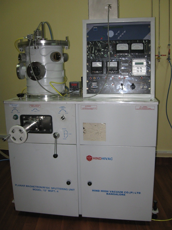
- Lab consist of a sputtering system for deposing the thin films of metals and insulators.
Device Characterization Section
- Consist of a CV ⁄IV measurement system, probe station, thin film thickness measurement system, wafer dicing machine and a wire bonder
Fabrication Lab has following facilities:
- Mask Aligner: SUSS MicroTec
- Vaccuum Spin Coating Unit
- Oxidation and Diffusion Furnace:ThermCo Systems
- Keithely Semiconductor Characterization System
- RF/DC Sputtering Unit
- Thermal Vaccuum Coating Unit
- Profilometer: Ambios Technology
- Four-Point Probe System
- Chemical-Mechanical Polishing System (CMP)
- DI Water plant
- Chemical Bench
- Aneanling Furnace Developed in House
- Stirrer Hot Plate
- Atomic Layer Deposition(ALD) System (To be installed Very soon )
|
|