
ASIC Implementation of low power variable resolution ADC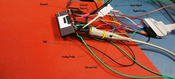 High resolution ADC dissipates high power and occupies large silicon area. A solution to save power in ADC is therefore to detect the current operating condition and vary the resolution accordingly. In this ADC design, resolution is dynamically adjusted according to the given channel conditions. The approach followed in saving power is done by switching some of the stages of the ADC to the standby mode (depending upon the input strength) where power dissipation is only due to the leakage current. The variable resolution ADC has been designed using Tanner tool on 500nm CMOS technology (AMIS_0.5_CFN kit) and chip is fabricated from MOSIS foundry. |
||||||